Advanced Functional Materials
Advanced Functional Materials




Rongming Wang Professor at the University of Science and Technology Beijing, Recipient of the State Council Special Allowance
Suhuai Wei Professor at the Beijing Computational Science Research Center, Member of the Thousand Talents Program / China’s Most Cited Researcher
Leo WM Lau Professor at the University of Science and Technology Beijing, Member of the Thousand Talents Program
Dongsheng Geng Professor at the University of Science and Technology Beijing, Member of the Thousand Youth Talents Program / China’s Most Cited Researcher
【Chief members】
Rongming Wang Professor at the University of Science and Technology Beijing
Suhuai Wei Professor at the Beijing Computational Science Research Center
Leo WM Lau Professor at the University of Science and Technology Beijing
Dongsheng Geng Professor at the University of Science and Technology Beijing
【Research Background】
Among the different fields in material science, the controllable synthesis of materials is the foundation of all research. A deep understanding of nanostructure growth on the characteristic scale is the cornerstone for controllable synthesis. Although transmission electron microscopy and other atomic-scale characterization methods are often used in conjunction with nanomaterial preparation methods to deduce the growth mechanism of nanostructures, characterization is often conducted after completion of the growth. However, this post-growth analysis technique does not reveal the real-time evolution of the nanostructures. By contrast, through a simulation of the physicochemical process of nanocrystal growth under environmental transmission electron microscopy (ETEM) combined with a spherical aberration correction, our team is able to observe the dynamic behaviors of atom migration as well as the evolutions of atomic and electronic structures at an atomic scale during nanocrystal growth, thereby providing direct experimental evidence for investigating the crystal growth mechanism and explaining the formation of a microstructure.
【Research Objectives】
Our team aims to establish a surface dynamic instrument cluster for the high-throughput preparation and characterization of low-dimensional functional materials as well as an in situ atomic-scale characterization system and technology for the multi-field coupling effect. The team also conducts high-throughput preparations and in situ characterizations of transition metals and their compound nanomaterials and heterojunctions. Combined with simulation calculations, the structure–performance relationship and performance optimization of these materials are investigated to promote the application of transition metals and their compound nanomaterials in multiple fields, such as electrocatalysis (including hydrogen and oxygen evolutions), gas sensing (such as hydrogen sensing), and solar cells.
【Main Research Areas】
1. Determination of the regulation and in situ characterization of the growth and structure of low-dimensional functional materials.
2. Atomic-scale structural evolution characterization and defect manipulation of materials under an ambient atmosphere and multi-field coupling.
3. High-throughput calculations of the structural and performance evolutions of the material under stimulated ambient atmosphere and operating conditions.
【Significant Research Progress】
Atomic-scale in situ characterization of material nucleation, growth, and reaction processes under multi-field coupling
Utilizing ETEM with a spherical aberration correction (FEI Titan ETEM G2), we have established an in situ characterization platform to characterize the nucleation, growth, and structural evolution of materials with atomic spatial and millisecond time resolutions. Based on this platform, we developed a quantitative electron microscopy method to characterize the displacement of atomic structures at a pm resolution, as well as a method to characterize the three-dimensional atomic structure of materials with a complex structural system. In addition, we conducted multiple exploration studies on the in situ characterization of the controlled synthesis, structural evolution, and reaction processes of materials under multi-field coupling conditions such as the temperature field, ambient atmosphere (Ar, N2, CO, CO2, H2, CH4, etc.), and electron beam irradiation. From the experiments, we observed the rotation and surface atomic migration behaviors of Au nanoparticles on the surface of MoS2, as well as the accelerated preferred orientation and aggregation growth of Au particles under electron beam irradiation, forming an epitaxial alignment of Au dendrites on MoS2 [Nano Research 12 (2019) Doi://10.1007/s12274-019-2329-4].
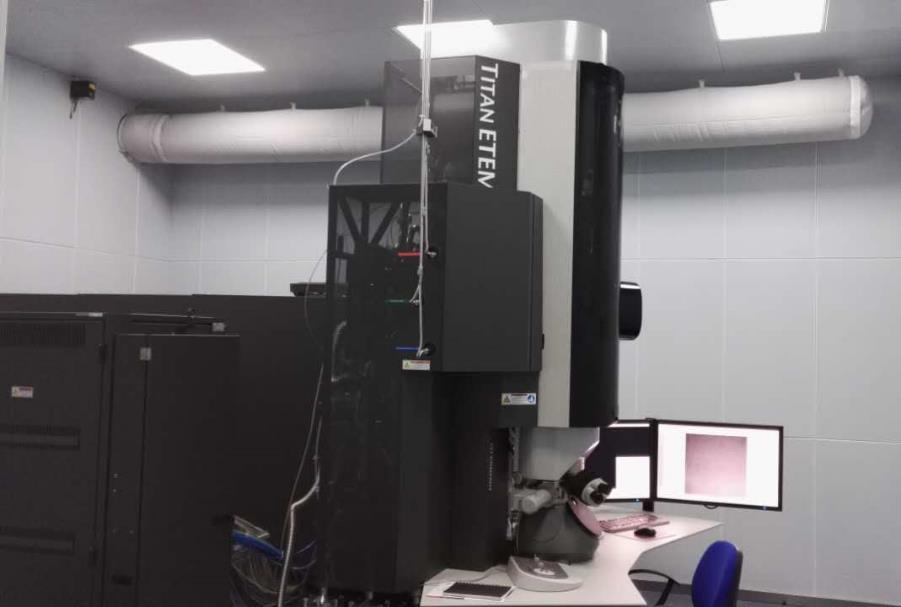
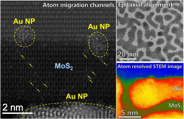
Fig. 1 Left: In situ characterization platform based on ETEM with correction of spherical aberration. Right: Accelerated preferred orientation and aggregation growth of Au particles under high-energy electron beam irradiation.
2. High-throughput material preparation system and technology based on surface dynamic instrument cluster
Based on the instrument cluster theory, we integrated advanced surface chemical composition and electronic structure regulation instruments with state-of-the-art surface chemical and physical characterization instruments to form a new multi-function instrument cluster, which is a major breakthrough in the development of scientific instruments. By doing so, an integrated atomic layer deposition (ALD) technology has been primarily established, which combines a supra-thermal particle system with an XPS surface dynamic instrument cluster system. Therefore, high-throughput preparation and the in situ characterization of low-dimensional functional materials can be conducted, where samples can be directly transferred to the XPS system for in situ characterization without being affected by the external environment. These achievements have provided further insights into the structure and physical property relationship of transition metals and their compound nanomaterials, and are playing a positive role in improving the independent design and manufacturing capabilities of scientific instruments in China.
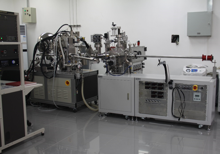
Fig. 2 Surface dynamic instrument cluster system
